China’s Chip Packaging Boom: Homegrown Firms Race Ahead of Global Rivals
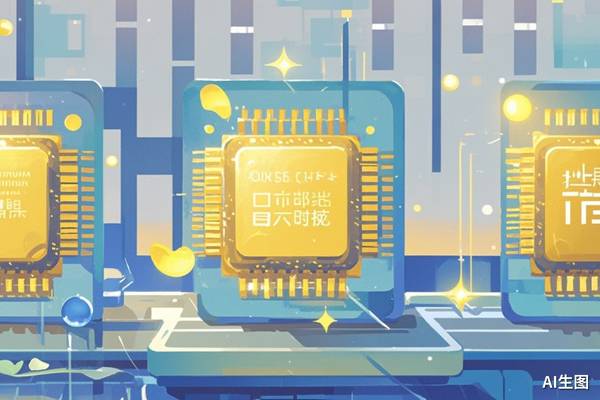
Chinese chipmakers are accelerating their push into high‑end advanced packaging, a move that could reshape the global semiconductor landscape. Tongfu Microelectronics has begun mass‑producing flip‑chip packages with high yields and has filed an AI‑focused packaging project in Nantong, positioning itself for the lucrative AI accelerator market. The company also announced a breakthrough in co‑packaged optics (CPO), with early reliability tests passed and further development tied to customer demand. At the same time, Huatai Technology is leveraging its integration expertise to break into the premium new‑energy‑vehicle sector, while new partnerships with AI firms open fresh growth avenues. The surge in large‑model AI and the rollout of smart cars are driving stricter requirements for chip performance, power efficiency and integration density, making 2.5D/3D, fan‑out and CPO packaging essential. Domestically, leaders like JCET have built a full‑stack packaging portfolio—covering wafer‑level, SiP, flip‑chip and wire‑bonding—to serve AI, automotive, HPC and networking applications. Their CPO solution merges optical engines with compute ASICs, slashing bandwidth bottlenecks and boosting energy efficiency. Internationally, ASE remains a frontrunner in fan‑out panel‑level packaging, planning AI‑GPU production on 600 × 600 mm panels by 2026, while giants such as Marvell and MediaTek consider Intel’s EMIB technology. These advances not only fuel the growth of Chinese chip firms but also reduce reliance on foreign packaging tech, pushing China’s semiconductor chain toward the high‑end tier and reshaping the competitive dynamics of the global market.
Read more