Tiny 0.42‑Nanometer Trick Could Supercharge Future Computer Chips
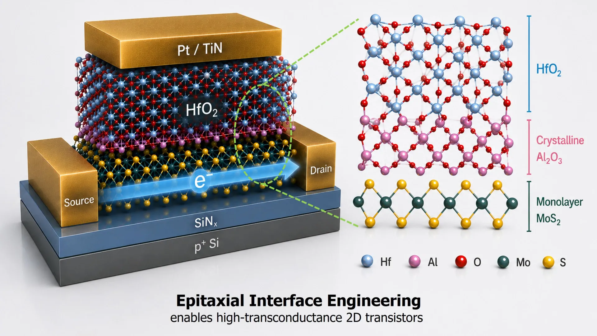
Researchers at National Yang Ming Chiao‑Tung University have discovered a way to make transistors— the tiny switches that power every electronic device—much smaller and more efficient than today’s silicon‑based designs. By engineering an ultra‑thin, 0.42‑nanometer‑wide atomic layer at the junction between a semiconductor and its insulating material, they created a protective “bridge” that lets electrons flow smoothly while keeping the insulating layer extremely thin. This delicate balance gives the new transistors strong electrical control and high performance, something that has been hard to achieve with atomically thin materials. The team used a chemically grown monolayer of molybdenum disulfide (MoS₂) instead of hand‑picked flakes, a step that brings the technology closer to large‑scale, wafer‑level production. The breakthrough could pave the way for chips that are not only faster and more power‑efficient but also dramatically smaller, opening new possibilities for everything from smartphones to advanced AI hardware. While still in the research stage, the findings suggest a shift in how engineers think about designing the next generation of microprocessors, moving beyond the limits of traditional silicon.
Read more